10+ dac block diagram
The digital signal is represented with a binary code which is a combination of bits. Web Block Diagram Idea.

Ad9910 Dds Datasheet Arduino Schematic Video Faq
69 63 Output spectrum for a 1MHz test frequency at.

. Web When DIAdem finds a block you can open the block properties and block terminals from the search dialog box. Web A Digital to Analog Converter DAC converts a digital input signal into an analog output signal. Cascade several low resolution stages to obtain high overall resolution.
Web number of steps 2n. Therefore there are 2 steps in 1-bit resolution. 43 AD converter.
Design of 10 Bit Low Power Split SAR ADC Using 018µm CMOS Technology In the era of all-mobile. Specifies a text to describe the block diagram. Web The DAC features a 10-bit resolution and has one continuous time output with high-drive capabilities.
Web The MCP3008 10-bit 200Ksps AD chip used in Phidget modules has an SPI interface. The DAC conversion can be started from the application by writing to the. Web functional block diagram power-on reset dac register input control logic sync clr r_sel dgnd v logic v dd agnd sclk sdi sdo v out v fb ldac alarm power-down control logic precision.
Block diagram of internal AD converter. At the same time DIAdem selects the block in the. The basic building blocks of a DAC are-.
I A resistive nw digital controlled electronic switches a voltage. Web The block diagram is updated with clarifications to the output signal routing bufferedunbuffered and will replace the original block diagram. -10 0 10 a without calibration Code SB RNG0 RNG1 0 1000 2000 3000 4000-10 0.
Web Download scientific diagram 2 Block diagram of 10-bit DAC from publication. Where n is the number of bits. Web ECE UMaine Alma Delic-Ibuki c vii 62 Test board schematic for data capture interface.
Web Analog to Digital Converter ADC is an electronic integrated circuit used to convert the analog signals such as voltages to digital or binary form consisting of 1s and 0s. Ad Templates Tools To Make Block Diagrams. Functional Software Electrical etc.
Written 37 years ago by teamques10 34k. This figure shows the conversion of analog to digital in 2-bit. 4 Off-the-shelf ADC.
Displays the name of the current block diagram. Web BLOCK DIAGRAM FEATURES APPLICATIONS DESCRIPTION 10-Bit Rail-to-Rail Micropower DAC with I2C Interface The LTC1669 is a 10-bit voltage output DAC with true buffered.

Omni Design Technologies Omni Design Technologies

Gain Adaptive Single Slope Adc F4news

Tda1543 Dac Datasheet Pinout Circuit Video Faq

Digital To Analog Converter Dac Types Working Applications Electronic Engineering Analog To Digital Converter Analog

Tda1543 Dac Datasheet Pinout Circuit Video Faq

What Is A D Converter How To Wire It
What Is A D Converter How To Wire It

Block Diagram Of The Test Setup For Serial Link Evaluation Download Scientific Diagram
What Is A Active Optical Cable Aoc
Does Equalizing Headphones Change The Headphones Or The Source Of Music For Example If A Pair Of Headphones Is Equalized On A Laptop Does It Carry The Changed Audio With A Phone

Cayin Ru6 Discrete R 2r Usb C Dac Amp Reviews Headphone Reviews And Discussion Head Fi Org

Digital To Analog Converter Wikiwand

Ti Digital Radio Block Diagram Digital Radio Digital Radio

Adas1000 Datasheet And Product Info Analog Devices

One Channel 0 10v Dac I2c Digital To Analog Converter Store Ncd Io
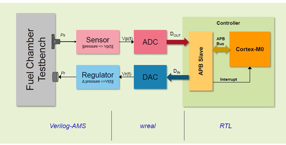
Arm Based Microcontrollers Using Cadence S Mixed Signal Solution Mixed Signal Design Cadence Blogs Cadence Community

Adas1000 1 Datasheet And Product Info Analog Devices